Just for fun, I've been fiddling with the 6502's instruction grid, putting stuff in that I might like to have in some fantasy '65C20'.
To start with, I'll give it most of the 65C02's additions, with the same opcodes:
BAL #rel (aka BRA); BAL ##rel (aka BRL); TSB &; TSB &&; TRB &; TRB &&; BIT #; BIT &,X; BIT &&,X; JMP (&&,X); STZ &; STZ &,X; STZ &&; STZ &&,X; PHX; PHY; PLX; PLY; INC A; DEC A.
Next up, for Group 2 (where LDX # and BAL ##rel live) I'll have a relative word addressing mode, completing the existing short branches: BPL, BMI, BVC, BVS, BCC, BCS, BNE and BEQ ##rel, sharing the same high nibble as their short counterparts. There's BSR - the relative word equivalent of JSR to aid relocation - as well as PHM ## and PHM ##rel (push memory to stack), CPB # and LDB #.
B is an 8-bit register that is mainly used as a 'bit on the side', so you don't have to stack quite so much. It's also used with so-called Long Mode, which replaces Decimal Mode (which I don't think was used much) and treats A and B as a combined BA register for the purpose of maths and logic instructions on A. CLD and SED are likewise replaced with CLL and SEL.
There's an 8-bit D register (Direct Page) which needs no introduction.
There's also an 8-bit E register (Extended Addressing). We put the 6502's three unconnected pins to use and repurpose the SO pin to create a 20-bit address space. The E register's nibbles define the current 'Near' and 'Far' bank.
Complementing this are new addressing modes which cause the Far bank to be emitted, rather than the Near bank.
The far addressing modes use the ORA set of instructions (ORA, AND, EOR, ADC, STA, LDA, CMP and SBC), applied to groups 3, 7 and F, such that:
* Group 3's instructions each get (&),E and (&),X,E addressing modes.
* Group 7's get &,E and &,Y,E addressing modes.
* Group F's get &&,E and &&,X,E addressing modes.
Now, if the Near and Far banks are different, the programmer has access to a second 64kb bank via those instructions. In addition, the JML (&&) instruction works the same as JMP (&&) except it swaps the near and far banks, after it has loaded the vector but before it has loaded the true address it's pointing to.
Here's the kinky bit... if the Near and Far banks are the same, the ISA effectively becomes more orthogonal. E.g. you now have: LDA #; LDA (&); LDA (&,X); LDA (&),X; LDA (&),Y; LDA &; LDA &,X; LDA &,Y; LDA &&; LDA &&,X; LDA &&,Y
Next up, BRK has its own vector, so no need to mess about testing the stack.
There's also a SWI instruction which is the same as BRK except it has a different vector again. This makes syscalls more viable. In particular, the D register can be used to point to a page-aligned parameter block, which will speed OSWORD-style ISRs.
There are two stack pointers; one for bank 0 (the System stack) and one for all other banks (the User stack). The S register exposes the stack pointer belonging to the current Near bank.
Pushing and pulling registers with PHx, PLx, JSR, BSR and RTS uses the User stack (or System if you're in bank 0). There is also PHB, PLB, PHD and PLD.
Hardware and software interrupts push E, PC and P to the System stack, set R, set E:=E >> 4 (i.e. setting Far to Near, and Near to 0) and vector to their ISR in bank 0. RTI pulls P, PC and E from the System stack, ofc.
R is another new flag in P, replacing the transient B flag. R is concrete. It is used to override bit 6 of the RTI opcode - when clear, the RTI becomes a BRK. R is cleared on reset, set when the CPU handles an interrupt (after it's pushed P), updated on RTI and otherwise read-only. This means 1) non-System banks can't mess with System stack data; 2) a System ISR can forward a request to firmware in another bank with effectively a 'this time only' RTI privilege.
R also controls access to E. When clear, E is read-only. Again, security... software in a non-System bank can only 'bust out' of its 64kb or 128kb space by issuing the relevant SWI. The ISR in bank 0 will then check its private process management data to check if that's allowed - meaning we have a part-hardware, part-software MMU solution, albeit with coarse granularity.
The unused '1' bit in P becomes the M flag (emulate enable). It is set on reset and once clear remains so until another reset.
Other additions, some nicked from the 65C816 (but sticking to 3 bytes max per instruction are: JMP (&); JMP (&,X); JSR (&); JSR (&,X) because I like the idea of further abstracting function tables with Direct Page; JSR (&&); JSR (&&,X) because how often have we wished we could do that?
There are new transfer instructions: TDA; TEA; TXY; TYX.
Plus, a set of SWAP instructions to help alleviate that constant Tower of Hanoi between registers! We have: SDA; SEA; SXY (uwu); SAB; SAX; SAY.
Finally, WAI, also nicked from the 65C816...
...and SEV!
I know, a dedicated MMU would help provide a more granular multi-process address space than the arrangement above. But the E-approach struck me as way to kill two birds with one stone. No need to have a full 64kb in a single bank, anyway. With 16 to play with, plus address translation circuitry to account for those 4 bank bits, you can spread your various resources out quite thinly and achieve granularity that way. E.g. bank 0 with its 16kb OS ROM and 2kb RAM; bank 1 for the paged filing system and 2kb of its own RAM; bank 2 for the paged language and 2kb RAM; bank 3 for the frame buffer; bank 4 for the user. Collectively, they need only a very small subset of the combined 1MB address space, so we can maximise use of the 16 available banks.
Fantasy 6502 variant...

Re: Fantasy 6502 variant...
Wow, seems like you have been thinking about this for a while!
There are a few of the 6502 undocumented op codes that I would like, plus some similar ones for Sprite drawing. Having a 16 bit accumulator would be good and the extra registers are always welcome.
I often find myself having:
Lda counter : beq done
Dec counter : bne done
...
. Done
Which feels like it could fit in a single instruction.
Faster pha and pla would be good as well as a combined pla:pha to just read the value at the top (bottom) of the stack.
Re: Fantasy 6502 variant...
Have you looked at the 68HC11 instruction set? It's very like the 6502 but it has some extra registers, addressing modes and instructions.

Re: Fantasy 6502 variant...
That's what I moved on to in the 90's after learning 6502 in the 80s'.
Unfortunately, HC11 is EOL but the closely related HC12 lives on as
the S12XE which has A+B(D) acculmulator and a heap of addressing
modes, page banked memory, supervisor mode.
I did a Tube port for it at one point.
Re: Fantasy 6502 variant...
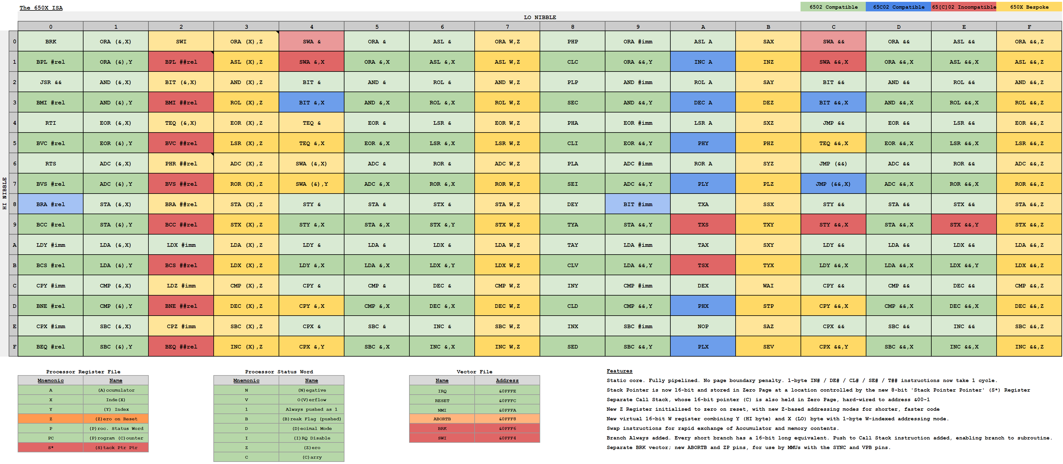
It's my week off and instead of working on the game, or anything much else for that matter, I've taken a fresh look at the 6502's ISA and fantasised. Whether I'll get around to learning about Verilog, FPGAs etc in order to sort of make it real, I don't know.

I started with the 65C02's instruction set, like before. I've kept the 16-bit relative branches, reusing the short opcodes, so that assemblers can abstract short vs. long away from the programmer.
I've also pinched the idea of making Z a writable register, initialised to zero on reset. Accompanying that is a set of Swap instructions, so that you can use Z as your 'bit on the side' when you need to juggle values around. This makes it easier and quicker to do 16-bit arithmetic and logic, and to have three indexes on the go at once.
Groups 7 and F contain interleaved combinations of arithmetic/logic and RMS instructions with the Y index. I figured that rather than invent a load of new instructions, why not try to make some of the existing ones a bit more orthogonal. I know orthogonal isn't everything but if you've got two index registers it makes sense to try to support them both as evenly as possible so that from-to logic is made simpler and quicker. Less Tower of Hanoi, more getting stuff done.
Since we have JMP (&&,X) let's also have JSR (&&,X) so that when one subroutine farms out work to various other (reusable) subroutines, we can still return to it afterwards so that it can do other stuff like restoring context before returning to the original caller.
BRK gets its own vector!
There's a SWI instruction which works like BRK, except its operand is used as an index into page &FE00 a la JMP (&&,X) enabling up to 128 (or more, if you can cunningly overlap) direct syscalls.
I've pinched the 6508's idea of implementing Zero Page as static RAM within the CPU. But here it's zero-turnaround RAM, so there are no bus access cycles that you'd otherwise get. To make the most of this, there are SWA & and SWA &,X instructions to exchange the contents of the Accumulator with the given Zero Page location. That brings Zero Page even closer to being, in effect, 256 registers.
Here's the kinky bit...
Since Zero Page is zero-turnaround static RAM inside the CPU, the indexed indirect and indirect indexed addressing modes now take the same number of cycles as absolute indexed. No more penalty for going indirect.
Exploiting this further, the Stack Pointer is now 16-bit and contained within Zero Page, at a location controlled by the new 'Stack Pointer Pointer' register (S*). Stack operations are therefore implicit indexed indirect loads and stores with index auto inc/decrement. The programmer can therefore have many different stacks on the go and block copies become a lot quicker. There is also a separate Call Stack, whose 16-bit pointer is also contained in Zero Page, at location &00. No more awkward mixing of data and addresses, so it's easier to do re-entrant subroutines.
In addition, doing a TSX means that (&, X) instructions access the end of the current stack. Aiding this further, the indexed indirect ALU instructions now have 'indexed indirect indexed' counterparts, i.e. (&,X),Y. Combined with Zero Page stack pointers, a special case of these instructions is stack-relative operations, analogous to those in the 65816 but more generalised and without having to gobble up all of Group 7 to do it.
Finally, there are Zero Page Access, Branch Wraparound and ABORT pins, for the benefit of MMUs.
I.e. if the CPU signals that the user is fiddling with something in ZP that they shouldn't, the MMU can signal an ABORT right back at it; this is a kludgy solution to the problem of not having all the RAM shielded by an MMU before the fact but providing the CPU abandons the current instruction on receiving an ABORT, rather than completing it and then servicing this interrupt, then the Zero Page Access pin serves as a notification of intent.
When the MMU is told about a branch wraparound, it can either ignore it, keeping the user in that same 64kb space, or it can ABORT, or it can switch the user into an adjacent space - it's up to the system designer.
Re: Fantasy 6502 variant...
This is one way to implement a fantasy 6502:
Quite technical video series (10 episodes) on implementing/emulating a 6502 in micro code with more things like interrupt handling to follow.
How to build a 6502 TTL-CPU: Part 1
Quite technical video series (10 episodes) on implementing/emulating a 6502 in micro code with more things like interrupt handling to follow.
How to build a 6502 TTL-CPU: Part 1
Re: Fantasy 6502 variant...
Ah, thank you. I have an electrical engineering friend who's looking into TTL stuff, so I'll pass that on to him as well.tricky wrote: ↑Mon Mar 25, 2024 7:23 pm This is one way to implement a fantasy 6502:
Quite technical video series (10 episodes) on implementing/emulating a 6502 in micro code with more things like interrupt handling to follow.
How to build a 6502 TTL-CPU: Part 1

Re: Fantasy 6502 variant...
Here were my thoughts on a 32-bit 6502, fitting into the existing opcode and mnenomic scheme:
https://mdfs.net/Docs/Comp/6502/32bit
One day I'll get around to finishing it, and may even update my Asm65, Dis65, and Em65 to implement it.
https://mdfs.net/Docs/Comp/6502/32bit
One day I'll get around to finishing it, and may even update my Asm65, Dis65, and Em65 to implement it.
Code: Select all
$ bbcbasic
PDP11 BBC BASIC IV Version 0.45
(C) Copyright J.G.Harston 1989,2005-2024
>_-
gordonDrogon

- Posts: 94
- Joined: Fri Nov 23, 2018 12:39 pm
- Location: Scottish Borders
- Contact:
Re: Fantasy 6502 variant...
There have been some interesting variants of the 6502/65c02 made in the past including a 32-bit version inside an FPGA (at least I think that's what it was). Some folks over on 6502.org have done weird stuff too...
And that's all good - and worthwhile if its your thing for a personal project - getting wider adoption is always a tricky thing to do...
One thing... I wonder if you're overlooking is the 65c816. I don't know if anyone has tried dropping one into a Beeb but I suspect the Beebs timing might require an adapter board for some signals, however it has a lot of what you need - a 16-bit Acc (and X and Y), direct page as well as a potential 24-bit address bus. I know that BBC Basic 4 will run on an '816 in C02 emulation mode (as I do it on my own '816 SBC) but the OS vectors need relocating as they clash with the hardware vectors on the '816 - so think about that if you want to maintain a degree of compatibility... (I patch the BBC Basic and Comal ROM images to make them work but others evade my patching algorithm and won't work)
The downside I've found after making and using my own '816 system is that it's not always as easy to write code for as the '02 so that may be a consideration if this every gets past the drawing board... There are some irritating (to me) anomalies too - e.g. trying to load an 8-bit value when in 16-bit memory mode loads a 16-bit value - which might be fine, but it wastes a cycle then you need to mask off the top byte which wastes another 3 cycles... critical when this is the fetch/dispatch loop of a bytecode VM (which is the core of my '816 system)
There are always going to be compromises like this though and one persons instruction of joy may well end up being another instruction of pain, so until you actually sit down and write the sort of code you want to write then who knows...
Cheers,
-Gordon

Re: Fantasy 6502 variant...
But
In general I do believe that writing an emulator for a new or revised architecture is a very rewarding and informative step.Your search - site:mdfs.net "em65" - did not match any documents.
Running such an emulator as an application on the Native ARM copro in PiTubeDirect would be a nice retro way to do it.
Re: Fantasy 6502 variant...
Interesting thoughts on a 32-bit 6502... one could argue that a binary incompatible version is basically the ARM1 but it's interesting to explore how to extend the 6502 in various ways whilst preserving compatibility with the original ISA.
My own avenue of interest is seeing just how far the 6502's original 8/16-bit ISA could be optimised in a way that sticks to those widths. It occurred to me since I drew that previous opcode grid that the addition of a (writeable) Z register could really help with that, more so than I've seen in the 65CE02:
Those Group 3 and 7 instructions are all 1 byte in length because they get their base address from a register rather than an operand in main memory. That saves 1 byte and 1 cycle in the case of Group 3, which helps compensate a tad for indirect addressing's increased cycle count. The saving is 2 bytes and 2 cycles for Group 7... whereas an LDA abs,X takes 4+ cycles, an LDA W,Z would likely need only 2+ cycles. Or just 2 if we can ditch the page boundary penalty, which iirc the 65CE02 did manage. Combine that with register IN/DE operations requiring just 1 cycle and we're on course for having code that run 2-3 times faster at the same clock speed.
Poking around in a stack remains simple, since S is now S* (the 'Stack Pointer Pointer') and acts as a 1-byte address in Zero Page where the true (16-bit) stack pointer lives, making it very similar in function to the Group 3 loads and stores. There IS a cycle penalty here, though, since obvs it'd need to load that pointer, adjust it, read/write the value pointed to, and also write the adjusted pointer value back... having Zero Page as zero-turnaround SRAM inside the CPU itself would probably partly or wholly claw those cycles back but it does create a big abstraction inversion problem for MMUs. Still chewing this!
STZ is out, since we can make plenty of savings elsewhere with those far more generalised 1-byte instructions.
TSB and TRB are out... frankly coz they seem a tad idiosyncratic. Some of the SWA variants take their place. Complementing BIT/AND we have TEQ/EOR since TEQ is to EOR as BIT is to AND.
Nicked from the 65C816 is PHR which pushes a 16-bit value to the Call Stack, computed as an address relative to PC. It's the next best thing to having a full set of conditional 8 and 16-bit Branch, Saving Return Address and why I ditched JSR (&&,X).
Re: Fantasy 6502 variant...
Because I just can't let it go...
I do wonder how much of a speed boost this thing could provide. E.g. those group 7 instructions, 1 byte in length but providing 16-bit absolute addressing via the YX (W) register. Combine that with INW and DEW instructions that take care of wraparound for you. I'm going to have to have a crack at learning more about the physical internals and Verilog... hopefully there are sufficiently cheap FPGAs that can mount like DIPs to a breadboard!
I do wonder how much of a speed boost this thing could provide. E.g. those group 7 instructions, 1 byte in length but providing 16-bit absolute addressing via the YX (W) register. Combine that with INW and DEW instructions that take care of wraparound for you. I'm going to have to have a crack at learning more about the physical internals and Verilog... hopefully there are sufficiently cheap FPGAs that can mount like DIPs to a breadboard!
Re: Fantasy 6502 variant...
Actually... if the W register were ZY, then whenever Z=0 you'd effectively have &&,Y addressing in the group F instructions - which half of them don't otherwise support.
Another thing, you could have something that monitors the 6502's SYNC pin and the contents of the data bus in order to determine which group the opcode belongs to... and if it's group F (conveniently %1111) then it could bank switch for the subsequent execution load/store only and/or while MLB is held low.
That 'far bank' could either be the same as the 'near bank', thus allowing you to produce &&,Y addressing on the read-modify-store instructions, or it could differ and provide you with direct access to another 64kb. These banks could either be hard-wired, to make the circuitry as simple as possible, or controllable with a memory-mapped register a la ROMSEL.
I suspect this methodology is atomic / interrupt-safe, too, since the choice of bank is scoped to the current instruction only and the 6502 always waits until the current instruction has finished executing.
And even if you didn't have W and merely duplicated one of the other instruction groups (say, group 1 or D) in group F, in an otherwise unaltered 65[C]02, you'd still be opening the door for a second 64kb for data. Or if opcode bit 0 is set, on receipt, then internally it clears bit 1, forcing group 3 -> 1, 7 -> 5, B -> 9, F -> D. Meaning groups 1, 5, 9 and D have 'evil twins' 3, 7, B and F to the outside world, the 6502 suppresses (most) of the undefined instructions with no additional microcode, and the address circuitry can arrange a temporary bank switch when it spots an evil twin opcode being fetched.
That's your frame buffer sorted, for starters. And these group F instructions provide a certain degree of abstraction, too. The same code would access either bank, which would aid double buffering. An OS call would tell the program whether a second bank is present and provide a copy of the bank select register, so it knows what its group F instructions will be doing and work out how much leftover RAM there is for other stuff.
Re: Fantasy 6502 variant...
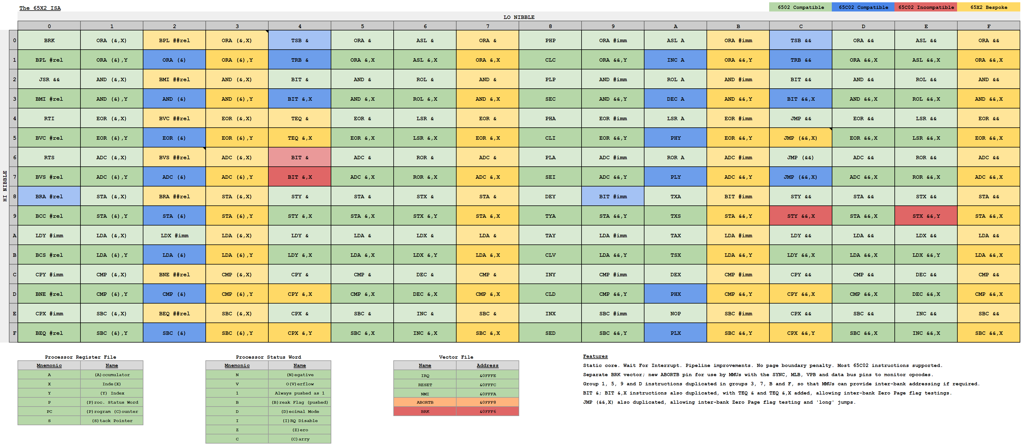
Something like this. Almost the same as the 65C02 except groups 3, 7, B, F are dupes of groups 1, 5, 9, D and a couple of other instructions are also duped.
If the MMU sniffs out one of these 'evil twin' group instructions, it bank switches for the duration of their data access.
BIT & and BIT &,X are also duplicated, so that you can check flags in the alternate zero page. TEQ & and TEQ &,X are included, to help that further.
JMP (&&,X) is also duplicated... this one is special because, if the system designer so chooses, the MMU could either switch banks before or after loading the PC with the new address (keeping it switched, obvs). Either way, it means we can execute code in either bank. But since this instruction lives in group C, it wouldn't be hard to limit its access to just the operating system!
-
dominicbeesley

- Posts: 2212
- Joined: Tue Apr 30, 2013 12:16 pm
- Contact:
Re: Fantasy 6502 variant...
Hello BigEd has just pointed me at this topic.
I've not had a chance to fully immerse myself in the ideas around the fantasy extended 6502 but it sounds like an interesting idea. As Ed says writing an emulator is always instructive - nothing like actually trying out the ideas. I also find that writing an assembler (and disassembler) can focus the mind on possible code sequences and improvements.
I've been working a lot recently on a 8/16 bit operating system and have a few items I would have liked but the 816 didn't quite provide:
Easier bank switches:
There seem to be a lot of code sequences like this
and even more awful swappery where data are being fetched from 3 or 4 and sent to others i.e. in the VDU drivers: constants, font, vdu variables, screen memory are all potentially in different banks. One solution might be to have different bank registers associated with X, Y register indexed address modes? Another solution might be to have an ldb n,S mode to quickly flit between bank registers?
Register size Modes
I've not much to suggest here other than the switchable modes are real pain in the butt to debug! The prefixes/suffixes on the 6809/6309 may be wasteful of cycles but they're much nicer to work with! I'm half tempted to look a developing a new assembler or maybe a pre/post assemble script to allow decoration of procedures with expected .a8/16, .i8/16, .far qualifiers and check that the caller is in the correct mode/using the correct jsr/jsl/jmp/jml. I'd also like something that kept track of where the DP pointer is and be able to define zero page offsets that are only allowed to be used when DP has the relevant value.
Temporary size swap prefix
It would be nice to have a prefix byte that allowed the current mode to be swapped for the following instruction. As gordon noticed loading an 8 bit value can be a pain when in 16 bit mode requiring multiple instructions
One thing you mention is having zero-page on-die and the indirected stack pointer. I'd say one of the things on the 65816 that I really like is to be able to redefine DP. It's used heavily in the Communicator MOS (and my prototype OS): private workspace for modules, private workspace (along with stack) for co-routines/threads/processes, stack frame pointer BP base pointer.
A simple adaptor I did in 2013:
viewtopic.php?t=6631
This plugs into the CPU socket and is really more like a 65802 IIRC - no extra memory. I had some fun with this and hacked around with an "improved" (i.e. slightly faster, slightly more buggy) Basic IV. I never got this to work reliably but I suspect it was really close I just didn't have the best test equipment at the time, also the BBC Micro I was using at the time was less than reliable.
A Tube version I did in 2015:
viewtopic.php?t=9975
This used the DE0 nano as the Tube ULA (I had nothing else to use at the time) and worked quite reliably despite it being a rather dodgy looking home-etched circuit board. I really ought to have a revisit of this and incorporate Hoglet's latest Tube stuff and make a proper board.
This is now included, I think, in the latest B-em iterations though I don't think it is cycle accurate but will run the same code.
Beeb816
https://github.com/BigEd/beeb816
http://forum.6502.org/viewtopic.php?f=4&t=6713
viewtopic.php?t=20752
Not one of mine, this is by BigEd, Hoglet and Rev
This is an in the cpu socket upgrade with extra RAM and an old-school CPLD doing the glue. It has quite clever clock-switching between the motherboard clocks and the faster 65816 clock and is built for performance.
Blitter Mk.1/2/3
viewtopic.php?p=329201#p329201
https://github.com/dominicbeesley/blitter-vhdl-6502
https://github.com/dominicbeesley/blitter-65xx-code
The Blitter project started out as me seeing what a BBC Micro would have been like with an expanded chipset (think Commodore Amiga). But has always had provision for using a 65816 as the CPU in a beeb. It provides a load of extra memory and some extended sound/graphics/memory shifting features. This was intended to be something for more general release but the chip shortage put paid to that. I still can't get hold of the Intel MAX 10 chips at a sensible price...we have been looking at alternatives using the cheap Chinese alternatives but these seem to be either hobbled with paid development tools (Efinix) or not readily available in small quantities other than on dev-boards (Gowin)
Model C
This is nothing tangible beyond a keyboard pcb so far but I've been building up (on the Blitter boards) to a more ambitious project - a Model C beeb.
- better graphics (more modes/more colours in existing modes, hardware sprites, etc, hdmi output)
- "chipset" features from the Blitter
- 65816 as main CPU, switchable to soft-core T65 for games compatibility
Communictor BASIC
viewtopic.php?t=21159&start=120
https://github.com/dominicbeesley/CommunicatorBasic100
This is a reassembly of the BASIC included on the Communictor in the 1.00 romset. It can be rebuilt to run on the Blitter boards, Beeb816 and Tube, including B-em
The main features of this BASIC are that it can load very large programs and have lots of data though the penalty is that it doesn't run quite a quickly as 65c02 BASIC IV (the cost of using 24 bit pointers for all parsing). It also includes a 65816 assembler
Model C MOS
https://github.com/dominicbeesley/model-c-mos
This is very much proof-of-concept. The idea is to try and make a 16/24bit operating system to run on the Blitter/Model C/beeb816 that provides maximum backwards compatibility with older BBC software. So far there are basic VDU drivers and some of the start up code. The interesting stuff is all about how the OS vectors will work. The aim is to have native programs be able to make use of older filing system ROMs seamlessly older BBC programs access extended services.
The idea is that old extension ROMs (in particular filing systems) should run in emulation mode and new modules run in native mode. This means the OS vectors, service calls etc need to pop in and out of native mode. In emulation mode older software should see a memory layout very much like a Beeb but in native mode bank 0 is all RAM - this requires some fairly simple logic hanging off the "E" pin. The tricky bit is when a switch occurs between modes that the code is running in a shared memory area (currently usurping part of page B) and that stacks/interrupts are not corrupted during handover.
DeIce68k
https://github.com/dominicbeesley/DeIce ... /dev-65816
This is rather misnamed but is a tethered (serial) debugger for various CPUs including the 816. The 816 branch is "good enough" to assist me with debugging my OS but still often gets its knickers in a not when stepping over register size mode changes.
I've not had a chance to fully immerse myself in the ideas around the fantasy extended 6502 but it sounds like an interesting idea. As Ed says writing an emulator is always instructive - nothing like actually trying out the ideas. I also find that writing an assembler (and disassembler) can focus the mind on possible code sequences and improvements.
I've been working a lot recently on a 8/16 bit operating system and have a few items I would have liked but the 816 didn't quite provide:
Easier bank switches:
There seem to be a lot of code sequences like this
Code: Select all
	phb
	phk
	plb
	lda tblOfConstants,X
	plb
Register size Modes
I've not much to suggest here other than the switchable modes are real pain in the butt to debug! The prefixes/suffixes on the 6809/6309 may be wasteful of cycles but they're much nicer to work with! I'm half tempted to look a developing a new assembler or maybe a pre/post assemble script to allow decoration of procedures with expected .a8/16, .i8/16, .far qualifiers and check that the caller is in the correct mode/using the correct jsr/jsl/jmp/jml. I'd also like something that kept track of where the DP pointer is and be able to define zero page offsets that are only allowed to be used when DP has the relevant value.
Temporary size swap prefix
It would be nice to have a prefix byte that allowed the current mode to be swapped for the following instruction. As gordon noticed loading an 8 bit value can be a pain when in 16 bit mode requiring multiple instructions
One thing you mention is having zero-page on-die and the indirected stack pointer. I'd say one of the things on the 65816 that I really like is to be able to redefine DP. It's used heavily in the Communicator MOS (and my prototype OS): private workspace for modules, private workspace (along with stack) for co-routines/threads/processes, stack frame pointer BP base pointer.
There have been a number of 65816 projects over the past decade and a bit:gordonDrogon wrote: ↑Tue Mar 26, 2024 8:51 am
One thing... I wonder if you're overlooking is the 65c816. I don't know if anyone has tried dropping one into a Beeb but I suspect the Beebs timing might require an adapter board for some signals...
A simple adaptor I did in 2013:
viewtopic.php?t=6631
This plugs into the CPU socket and is really more like a 65802 IIRC - no extra memory. I had some fun with this and hacked around with an "improved" (i.e. slightly faster, slightly more buggy) Basic IV. I never got this to work reliably but I suspect it was really close I just didn't have the best test equipment at the time, also the BBC Micro I was using at the time was less than reliable.
A Tube version I did in 2015:
viewtopic.php?t=9975
This used the DE0 nano as the Tube ULA (I had nothing else to use at the time) and worked quite reliably despite it being a rather dodgy looking home-etched circuit board. I really ought to have a revisit of this and incorporate Hoglet's latest Tube stuff and make a proper board.
This is now included, I think, in the latest B-em iterations though I don't think it is cycle accurate but will run the same code.
Beeb816
https://github.com/BigEd/beeb816
http://forum.6502.org/viewtopic.php?f=4&t=6713
viewtopic.php?t=20752
Not one of mine, this is by BigEd, Hoglet and Rev
This is an in the cpu socket upgrade with extra RAM and an old-school CPLD doing the glue. It has quite clever clock-switching between the motherboard clocks and the faster 65816 clock and is built for performance.
Blitter Mk.1/2/3
viewtopic.php?p=329201#p329201
https://github.com/dominicbeesley/blitter-vhdl-6502
https://github.com/dominicbeesley/blitter-65xx-code
The Blitter project started out as me seeing what a BBC Micro would have been like with an expanded chipset (think Commodore Amiga). But has always had provision for using a 65816 as the CPU in a beeb. It provides a load of extra memory and some extended sound/graphics/memory shifting features. This was intended to be something for more general release but the chip shortage put paid to that. I still can't get hold of the Intel MAX 10 chips at a sensible price...we have been looking at alternatives using the cheap Chinese alternatives but these seem to be either hobbled with paid development tools (Efinix) or not readily available in small quantities other than on dev-boards (Gowin)
Model C
This is nothing tangible beyond a keyboard pcb so far but I've been building up (on the Blitter boards) to a more ambitious project - a Model C beeb.
- better graphics (more modes/more colours in existing modes, hardware sprites, etc, hdmi output)
- "chipset" features from the Blitter
- 65816 as main CPU, switchable to soft-core T65 for games compatibility
Communictor BASIC
viewtopic.php?t=21159&start=120
https://github.com/dominicbeesley/CommunicatorBasic100
This is a reassembly of the BASIC included on the Communictor in the 1.00 romset. It can be rebuilt to run on the Blitter boards, Beeb816 and Tube, including B-em
The main features of this BASIC are that it can load very large programs and have lots of data though the penalty is that it doesn't run quite a quickly as 65c02 BASIC IV (the cost of using 24 bit pointers for all parsing). It also includes a 65816 assembler
Model C MOS
https://github.com/dominicbeesley/model-c-mos
This is very much proof-of-concept. The idea is to try and make a 16/24bit operating system to run on the Blitter/Model C/beeb816 that provides maximum backwards compatibility with older BBC software. So far there are basic VDU drivers and some of the start up code. The interesting stuff is all about how the OS vectors will work. The aim is to have native programs be able to make use of older filing system ROMs seamlessly older BBC programs access extended services.
The idea is that old extension ROMs (in particular filing systems) should run in emulation mode and new modules run in native mode. This means the OS vectors, service calls etc need to pop in and out of native mode. In emulation mode older software should see a memory layout very much like a Beeb but in native mode bank 0 is all RAM - this requires some fairly simple logic hanging off the "E" pin. The tricky bit is when a switch occurs between modes that the code is running in a shared memory area (currently usurping part of page B) and that stacks/interrupts are not corrupted during handover.
DeIce68k
https://github.com/dominicbeesley/DeIce ... /dev-65816
This is rather misnamed but is a tethered (serial) debugger for various CPUs including the 816. The 816 branch is "good enough" to assist me with debugging my OS but still often gets its knickers in a not when stepping over register size mode changes.
-
dominicbeesley
- Posts: 2212
- Joined: Tue Apr 30, 2013 12:16 pm
- Contact:
Re: Fantasy 6502 variant...
PS: opcode tables in the posts above are illegible here it might be worth attaching them as a pdf as well as inline images?
Re: Fantasy 6502 variant...
I like the 256 bytes of zero page as an instant register file but
I never liked 16bit (internal reg size, ignore data bus width) processors: I think Motorola* and Acorn were right jump straight to a 32bit programming model with linear addressing (no banking in native mode...) and make the programmers life easier.
So perhaps your zero page could support 32bit linear address indiect (4zp bytes) like JG Harstons link .
I presume A becomes usuable as an 8bit or 32bit entity (what about 16bit manipulations). Support for 24bit (3byte) addresses saves memory but architecturily expensive/limiting/odd..?
The 65816 approach to position independant code seems rather involved/ programnmer unfriendly compared to just having it as an extra addressing mode on suitable instructions?
*they regretted not making the 68008 ftom the start thus losing the Ibm pc to the Intel 8088 with its cost saving 8 bit data bus .... An Ibm based on 6800x would have saved me indecision over a beeb successor..)
I never liked 16bit (internal reg size, ignore data bus width) processors: I think Motorola* and Acorn were right jump straight to a 32bit programming model with linear addressing (no banking in native mode...) and make the programmers life easier
So perhaps your zero page could support 32bit linear address indiect (4zp bytes) like JG Harstons link .
I presume A becomes usuable as an 8bit or 32bit entity (what about 16bit manipulations). Support for 24bit (3byte) addresses saves memory but architecturily expensive/limiting/odd..?
The 65816 approach to position independant code seems rather involved/ programnmer unfriendly compared to just having it as an extra addressing mode on suitable instructions?
*they regretted not making the 68008 ftom the start thus losing the Ibm pc to the Intel 8088 with its cost saving 8 bit data bus ....
Re: Fantasy 6502 variant...
Hiya. Thanks, this is interesting and underlines the different ways that one could extend the 6502.dominicbeesley wrote: ↑Mon Apr 08, 2024 12:39 pm Hello BigEd has just pointed me at this topic.
I've not had a chance to fully immerse myself in the ideas around the fantasy extended 6502 but it sounds like an interesting idea. As Ed says writing an emulator is always instructive - nothing like actually trying out the ideas. I also find that writing an assembler (and disassembler) can focus the mind on possible code sequences and improvements.
I've been working a lot recently on a 8/16 bit operating system and have a few items I would have liked but the 816 didn't quite provide:
Easier bank switches:
There seem to be a lot of code sequences like thisand even more awful swappery where data are being fetched from 3 or 4 and sent to others i.e. in the VDU drivers: constants, font, vdu variables, screen memory are all potentially in different banks. One solution might be to have different bank registers associated with X, Y register indexed address modes? Another solution might be to have an ldb n,S mode to quickly flit between bank registers?Code: Select all
	phb
	phk
	plb
	lda tblOfConstants,X
	plb
Register size Modes
I've not much to suggest here other than the switchable modes are real pain in the butt to debug! The prefixes/suffixes on the 6809/6309 may be wasteful of cycles but they're much nicer to work with! I'm half tempted to look a developing a new assembler or maybe a pre/post assemble script to allow decoration of procedures with expected .a8/16, .i8/16, .far qualifiers and check that the caller is in the correct mode/using the correct jsr/jsl/jmp/jml. I'd also like something that kept track of where the DP pointer is and be able to define zero page offsets that are only allowed to be used when DP has the relevant value.
Temporary size swap prefix
It would be nice to have a prefix byte that allowed the current mode to be swapped for the following instruction. As gordon noticed loading an 8 bit value can be a pain when in 16 bit mode requiring multiple instructions
One thing you mention is having zero-page on-die and the indirected stack pointer. I'd say one of the things on the 65816 that I really like is to be able to redefine DP. It's used heavily in the Communicator MOS (and my prototype OS): private workspace for modules, private workspace (along with stack) for co-routines/threads/processes, stack frame pointer BP base pointer.
There have been a number of 65816 projects over the past decade and a bit:gordonDrogon wrote: ↑Tue Mar 26, 2024 8:51 am
One thing... I wonder if you're overlooking is the 65c816. I don't know if anyone has tried dropping one into a Beeb but I suspect the Beebs timing might require an adapter board for some signals...
A simple adaptor I did in 2013:
viewtopic.php?t=6631
This plugs into the CPU socket and is really more like a 65802 IIRC - no extra memory. I had some fun with this and hacked around with an "improved" (i.e. slightly faster, slightly more buggy) Basic IV. I never got this to work reliably but I suspect it was really close I just didn't have the best test equipment at the time, also the BBC Micro I was using at the time was less than reliable.
A Tube version I did in 2015:
viewtopic.php?t=9975
This used the DE0 nano as the Tube ULA (I had nothing else to use at the time) and worked quite reliably despite it being a rather dodgy looking home-etched circuit board. I really ought to have a revisit of this and incorporate Hoglet's latest Tube stuff and make a proper board.
This is now included, I think, in the latest B-em iterations though I don't think it is cycle accurate but will run the same code.
Beeb816
https://github.com/BigEd/beeb816
http://forum.6502.org/viewtopic.php?f=4&t=6713
viewtopic.php?t=20752
Not one of mine, this is by BigEd, Hoglet and Rev
This is an in the cpu socket upgrade with extra RAM and an old-school CPLD doing the glue. It has quite clever clock-switching between the motherboard clocks and the faster 65816 clock and is built for performance.
Blitter Mk.1/2/3
viewtopic.php?p=329201#p329201
https://github.com/dominicbeesley/blitter-vhdl-6502
https://github.com/dominicbeesley/blitter-65xx-code
The Blitter project started out as me seeing what a BBC Micro would have been like with an expanded chipset (think Commodore Amiga). But has always had provision for using a 65816 as the CPU in a beeb. It provides a load of extra memory and some extended sound/graphics/memory shifting features. This was intended to be something for more general release but the chip shortage put paid to that. I still can't get hold of the Intel MAX 10 chips at a sensible price...we have been looking at alternatives using the cheap Chinese alternatives but these seem to be either hobbled with paid development tools (Efinix) or not readily available in small quantities other than on dev-boards (Gowin)
Model C
This is nothing tangible beyond a keyboard pcb so far but I've been building up (on the Blitter boards) to a more ambitious project - a Model C beeb.
- better graphics (more modes/more colours in existing modes, hardware sprites, etc, hdmi output)
- "chipset" features from the Blitter
- 65816 as main CPU, switchable to soft-core T65 for games compatibility
Communictor BASIC
viewtopic.php?t=21159&start=120
https://github.com/dominicbeesley/CommunicatorBasic100
This is a reassembly of the BASIC included on the Communictor in the 1.00 romset. It can be rebuilt to run on the Blitter boards, Beeb816 and Tube, including B-em
The main features of this BASIC are that it can load very large programs and have lots of data though the penalty is that it doesn't run quite a quickly as 65c02 BASIC IV (the cost of using 24 bit pointers for all parsing). It also includes a 65816 assembler
Model C MOS
https://github.com/dominicbeesley/model-c-mos
This is very much proof-of-concept. The idea is to try and make a 16/24bit operating system to run on the Blitter/Model C/beeb816 that provides maximum backwards compatibility with older BBC software. So far there are basic VDU drivers and some of the start up code. The interesting stuff is all about how the OS vectors will work. The aim is to have native programs be able to make use of older filing system ROMs seamlessly older BBC programs access extended services.
The idea is that old extension ROMs (in particular filing systems) should run in emulation mode and new modules run in native mode. This means the OS vectors, service calls etc need to pop in and out of native mode. In emulation mode older software should see a memory layout very much like a Beeb but in native mode bank 0 is all RAM - this requires some fairly simple logic hanging off the "E" pin. The tricky bit is when a switch occurs between modes that the code is running in a shared memory area (currently usurping part of page B) and that stacks/interrupts are not corrupted during handover.
DeIce68k
https://github.com/dominicbeesley/DeIce ... /dev-65816
This is rather misnamed but is a tethered (serial) debugger for various CPUs including the 816. The 816 branch is "good enough" to assist me with debugging my OS but still often gets its knickers in a not when stepping over register size mode changes.
I wonder if your Model C could have a fantasy 6502 variant as a second processor, with a 65C02 on the main board for 'legacy' stuff. The Tube protocol already supports the core MOS API, I think. Or perhaps flip it around and have the 'legacy' Beeb as a second processor, analogous to https://en.wikipedia.org/wiki/Mega_II
I'm with you on modes thing. I was toying with a 'Long Mode' flag in P but in the end felt it would introduce too much 'flag paranoia', like there is with the D flag in the NMOS 6502.
It's a curious one, the 65816... iirc the reason for its creation was essentially to be a CPU that could do 24-bit addressing whilst retaining backwards compatibility with the 6502, because that's what they wanted for the Apple IIgs. I think if one weren't saddled with the requirement for backwards compatibility, then the 68000 would have probably been the more natural choice. As it is, the 65816 is an 8/16-bit chip with some 24-bit stuff bolted on, and the downside as you folks say is that it's a bit fiddly to program as a result. That's why the direction I've been exploring is to try to optimise the 6502's existing 8/16 architecture. I've mostly kept in mind the "ah, if only it were easier to do x!" moments I've encountered from my own assembly language programming. But that's not stopped me pinching a few of its ideas, as you'll see below!
As for ways of enlarging the address space, I was looking at how those NC pins might be put to work. But I've recently decided to separate concerns and leave all that stuff to an MMU, since there's way more under the sun that an MMU could be designed to do compared to what little leftover scope there is in the CPU. E.g. a program in user RAM should not be able to access a paged ROM's contents directly. It's none of the program's business! Meanwhile, that program wants to have a big expensive screen mode without sacrificing its own memory. An MMU can kill two birds with one stone by monitoring the Program Counter and Data Pointer addresses being emitted on the address bus and having a From-To mapping table, so that any code between &0E00 and &7FFF that tries to access anything between &8000 and &CFFF, say, will 'see' the frame buffer instead... I think the C64 uses that sort of approach. In fact, doesn't the Master do something along these lines? Point is, this is just one of any number of methodologies, and the CPU needn't have to be aware of them - or indeed any code that it's running. No modes etc. OK, it doesn't solve the problem of wanting to be able to access any location in a 24-bit address space directly without having to fiddle about with any translation tables, 'extended addressing' registers, Harvard-like data vs code pages etc. but if that's the requirement of your application software, then it's worth considering an application processor and system architecture that supports direct 24-bit addressing from the ground up.
I've uhmmed and ahhed about Zero Page... on the one hand, if it were implemented on-chip as zero-turnaround SRAM, then it's possible the indirect addressing modes can be made to run in the same cycle count as the absolutes, due to shaving off the cycle that would have been needed to load the byte operand from main memory. But on the other hand, it's a terrible abstraction inversion if you've got an MMU in mind. I guess it depends, as always, on the requirement. So the present state of play is I've reverted Zero Page back to main memory... however, I'm thinking memory-map the Program Counter, System (call) Stack Pointer and User Stack Pointer (all 16-bit, btw!) to locations just beneath the CPU's hardware vectors. They still live inside the CPU, obviously, but they can be accessed with the full power of the instruction set. Memory-mapped registers is nothing new to the 6502 range, anyway. I've reinstated the Direct Page register, as that's clearly very much desired and I totally dig its value... and with PC, S and U all memory-mapped you can set D = &FF and do PC and Stack-relative addressing! Combined with the 16-bit branch instructions etc. it should now be possible to create position-independent code without much fuss.
Here's a summary of the extras I've currently got going:
- Processor Status Word is unchanged
BRK has its own dedicated vector
New SWI instruction; same as BRK but with its own vector, so that syscalls may be quicker and simpler (i.e. more viable)
New ABORTB interrupt and vector
New 8-bit Z register
New virtual W register, combining ZY, with INW and DEW instructions
New 8-bit Direct Page register, D
New Register-Memory and Inter-Register Swap instructions.
Stack Pointer is now the 16-bit System Stack Pointer, S
Separate 16-bit User Stack Pointer, U
S, U and PC are memory-mapped to page &FF, beneath the hardware vectors
Every branch now has 8-bit and 16-bit relative addressing modes
Groups 3, 7 and F instructions now implemented, interleaving the ALU and RMS instructions
Group 3 instructions have Indirect Non-Indexed addressing
New INW and DEW memory instructions for inc/decrementing 16-bit pointers in Direct Page; with Group 3, software stacks become trivial
Group 7 instructions are 1-byte 'Absolute Implicit' addressing (e.g. EOR W) for denser code and 2 fewer cycles taken; 'software blitting'
Group F instructions are 3-byte 'Absolute Word Indexed' addressing, using the W register.
Group 0
- BRA #rel
- SWI #sig
BPL ##rel
PHR ##rel
BMI ##rel
DEW &
BVC ##rel
INW &
BVS ##rel
BRA ##rel
BCC ##rel
BCS ##rel
DEW &,X
BNE ##rel
INW &,X
BEQ ##rel
- ORA (&)
ASL (&)
AND (&)
ROL (&)
EOR (&)
LSR (&)
ADC (&)
ROR (&)
STA (&)
STX (&)
LDA (&)
LDX (&)
CMP (&)
DEC (&)
SBC (&)
INC (&)
- SWP &
SWP &,X
BIT &,X
STW &
STW &,X
LDW &
LDW &,X
CPY &,X
CPX &,Y
- ORA W
ASL W
AND W
ROL W
EOR W
LSR W
ADC W
ROR W
STA W
STX W
LDA W
LDX W
CMP W
DEC W
SBC W
INC W
- BIT #imm
- INC A
DEC A
PHY
PLY
ONE
TWO
PHX
PLX
- SAX
INW
SAY
DEW
SXZ
PHW
SYZ
PLW
TXY
TXD
TYX
TDX
WAI
SXY
SAZ
SEV
- SWP &&
SWP &&,X
BIT &&,X
LDW &&
JMP (&&,X)
STY &&,X
CPY &&,X
CPX &&,Y
- STX &&,Y
- ORA &&,W
ASL &&,W
AND &&,W
ROL &&,W
EOR &&,W
LSR &&,W
ADC &&,W
ROR &&,W
STA &&,W
STX &&,W
LDA &&,W
LDX &&,W
CMP &&,W
DEC &&,W
SBC &&,W
INC &&,W
PHR &AllRTSHere
LDA &device_register
BIT #255
BNE handleBit7Set
BVS handleBit6Set
BEQ handleNothingSet
ROR A:BCS handleBit0Set
.allRTSHere
<continued>
I.e. all those subroutines conclude with an RTS which takes us to the end of all the different tests. Handy if we need them to be reusable / don't want them to have to know where to jump back to. An efficient CASE/SWITCH structure.
PHR also allows us to synthesise JSR (&&) and JSR (&&,X) with JMP (&&) and JMP (&&,X). Not as good as having the actual instructions but it's a very tight squeeze getting all these opcodes in and we get more flexibility with a separate PHR.
There are plenty of Swap instructions available, both between register and memory, and inter-register. This should compensate somewhat for what few registers there are. For instance, it becomes trivial to synthesise (&&,Y) and (&&),X because of the SXY instruction. It's also quicker and simpler to synthesise 16-bit arithmetic and logic operations.
That virtual W register is handy for quite a few reasons, it turns out. Not only does it give you 16-bit addressing in both implicit and absolute word indexed modes, it makes checking for underflow trivial. E.g. load W with &00FF. Use Y indexing to update your page but do a DEW instead of DEY. The N and Z flags are set according to W rather than Y, so a DEW + BPL loop is your underflow check. Simple!
W also readily lends itself to OSWORD and the like.
You can also recreate a form of immediate indexed addressing with &&,W by effectively swapping the roles of && and W. I.e. set W to the given base address and then && acts as your immediate index into it.
The Implicit Absolute mode (or whatever its proper name should be) provides all ALU and RMS instructions with an implicit addressing mode using W. So that's 2 cycles saved if you can use one of those instead of absolute indexed, which adds up to quite a saving if you have a a page or more of data to iterate through. A sort of software blitter? Good for block transfers, certainly, which iirc the Z80 is better at.
Finally, when Z=0, the &&,W addressing mode behaves like &&,Y which is otherwise not available for the RMS instructions.
As mentioned above, PC, S and U are all 16-bit and all memory-mapped into page &FF beneath the hardware vectors. So, you can either do an LDW to get one of their values at that point in time, or you can set D=&FF and do PC, S or U-relative addressing, without having to invent 'd,S' or '(d,S),Y' groups of instructions. We can instead make stack-relative addressing a special case of something more general and therefore get more value out of the limited free opcodes available.
P.S. TXS and TSX are no longer necessary due to the above. Taking their place are the 'ONE' and 'TWO' instructions, which load but ignore the following one or two bytes. Many, many use cases, of course, including instructing any coprocessor or MMU that may be sniffing the CPU's pins.
Re: Fantasy 6502 variant...
If the Mega ii only needed a 6502 and some ram access , a 1 mhz plain 6502 was presumably cheap enough thay the GS might as well as had a nicer processor than the 65816 like a 68000... which I suppose might make it be labelled as a Woz macArx wrote: ↑Tue Apr 09, 2024 5:11 pmHiya. Thanks, this is interesting and ... The Tube protocol .... Or perhaps flip it around and have the 'legacy' Beeb as a second processor, analogous to https://en.wikipedia.org/wiki/Mega_IIdominicbeesley wrote: ↑ ...
.....
-
gordonDrogon
- Posts: 94
- Joined: Fri Nov 23, 2018 12:39 pm
- Location: Scottish Borders
- Contact:
Re: Fantasy 6502 variant...
I've often wondered about this - especially as (according to the timelines on wikipedia) the Acorn Communicator was released before the IIgs ...
I might have thought one way to "expand" it might be to invest in a bytecode of some sort - Sweet16 springs to mind and I've used that lot in the past on some 6502 projects but there is also Acheron - http://acheronvm.github.io/acheronvm/I think if one weren't saddled with the requirement for backwards compatibility, then the 68000 would have probably been the more natural choice. As it is, the 65816 is an 8/16-bit chip with some 24-bit stuff bolted on, and the downside as you folks say is that it's a bit fiddly to program as a result. That's why the direction I've been exploring is to try to optimise the 6502's existing 8/16 architecture. I've mostly kept in mind the "ah, if only it were easier to do x!" moments I've encountered from my own assembly language programming. But that's not stopped me pinching a few of its ideas, as you'll see below!
And I think I have given up on the '816 now - having written far too much code for it now. Mostly a 32-bit bytecode VM which overcomes the banked memory issues to present a nice 32-bit interface - at the expense of speed obviously. I achieve an effective clock speed of about 200-300Khz on a 16Mhz '816 CPU and most of the cycles "wasted" are to do with the '816s way of reading a byte from RAM when in 16-bit mode.
And of-course, having PiTube does make it easy to make your fantasy come true by writing it in C or ARM and running it as a co-pro...
Cheers,
-Gordon
Re: Fantasy 6502 variant...
The 65816 was originally going to be used in the Apple IIx, which was effectively the predecessor to the IIGS, already being designed as early as 1983:gordonDrogon wrote: ↑Tue Apr 09, 2024 9:19 pmI've often wondered about this - especially as (according to the timelines on wikipedia) the Acorn Communicator was released before the IIgs ...
"10-The Apple IIGS"
It seems like WDC had issues making the chip, however, which were perhaps resolved eventually by expertise at the various second sources. The 65816 variant in the Communicator was made by GTE, for instance. The IIGS was instigated or catalysed by Steve Wozniak when he returned to Apple after his leave of absence in the early 1980s, leaving plenty of time for others to use the 65816 before Apple finally did.
There was some previous discussion of such matters.
Re: Fantasy 6502 variant...
Ah, thank you. That's an interesting article. Yeah, the politics of the time... all that focus on the Apple /// compared to what a souped-up ][ might have been. Though its OS sounds good.paulb wrote: ↑Tue Apr 09, 2024 11:11 pmThe 65816 was originally going to be used in the Apple IIx, which was effectively the predecessor to the IIGS, already being designed as early as 1983:gordonDrogon wrote: ↑Tue Apr 09, 2024 9:19 pmI've often wondered about this - especially as (according to the timelines on wikipedia) the Acorn Communicator was released before the IIgs ...
"10-The Apple IIGS"
It seems like WDC had issues making the chip, however, which were perhaps resolved eventually by expertise at the various second sources. The 65816 variant in the Communicator was made by GTE, for instance. The IIGS was instigated or catalysed by Steve Wozniak when he returned to Apple after his leave of absence in the early 1980s, leaving plenty of time for others to use the 65816 before Apple finally did.
There was some previous discussion of such matters.
Incidentally, I love the feature in the GS graphics that 'holds' a particular colour in order to hardware-accelerate flood fills. A close relative / special case of Hold-And-Modify?
-
ThomasHarte
- Posts: 567
- Joined: Sat Dec 23, 2000 5:56 pm
- Contact:
Re: Fantasy 6502 variant...
There are some good ideas in there* — another is automatic dithering in 640px mode; in that 2bpp mode output colour actually comes from the 16-colour palette as two bits from the screen data plus two bits counting the output column. I've read that the original Apple monitors applied analogue mixing so as to combine adjoining pixels in that mode but never quite found out exactly what that function is. It definitely doesn't result in output as though the pixels were weighted equally, so it's quite a bit more interesting than it might have been.
Sadly the rest of the architecture is a mess, with even the official documentation referring to its support for Apple II-style memory paging as "the quagmire state". It also puts all video memory, regardless of mode, behind the 1Mhz bus so all video output is slow and there are no sprites, no hardware scrolling, not even a programmable start address. That's even without inevitably catty comments about the quality of the 65816 as a whole.
If you want to really, really appreciate the Archimedes, look at the IIgs for a how-not-to-do-it comparison.
* though the idea for hardware accelerated flood fills was basically Woz saying "if I implement this, even though the problem sounds really hard, I'm sure a smart software person will be able to exploit it for arbitrary 3d". But mostly it's just used by demoscene people who can precompute.
Re: Fantasy 6502 variant...
I'll have to have a look into the mechanics of that dithering, as I've been thinking about a fantasy video display chip, too. E.g. pipelining the video bytes and shifting the most significant bit of the 'next' into the least significant bit of the 'current'. A 16-bit shift register, I suppose, that loads the next low byte every 8 shifts. I suspect that alone would open the door to some additional nifty tricks for spoofing a high-res, high-colour mode.ThomasHarte wrote: ↑Mon Apr 15, 2024 4:30 pmThere are some good ideas in there* — another is automatic dithering in 640px mode; in that 2bpp mode output colour actually comes from the 16-colour palette as two bits from the screen data plus two bits counting the output column. I've read that the original Apple monitors applied analogue mixing so as to combine adjoining pixels in that mode but never quite found out exactly what that function is. It definitely doesn't result in output as though the pixels were weighted equally, so it's quite a bit more interesting than it might have been.
Sadly the rest of the architecture is a mess, with even the official documentation referring to its support for Apple II-style memory paging as "the quagmire state". It also puts all video memory, regardless of mode, behind the 1Mhz bus so all video output is slow and there are no sprites, no hardware scrolling, not even a programmable start address. That's even without inevitably catty comments about the quality of the 65816 as a whole.
If you want to really, really appreciate the Archimedes, look at the IIgs for a how-not-to-do-it comparison.
* though the idea for hardware accelerated flood fills was basically Woz saying "if I implement this, even though the problem sounds really hard, I'm sure a smart software person will be able to exploit it for arbitrary 3d". But mostly it's just used by demoscene people who can precompute.
P.S. Yeah, the original Archimedes is a masterpiece of minimalism, imho.
-
ThomasHarte
- Posts: 567
- Joined: Sat Dec 23, 2000 5:56 pm
- Contact:
Re: Fantasy 6502 variant...
It is definitely not that sophisticated; the complete implementation in my emulator to serialise a single byte of input is:Arx wrote: ↑Mon Apr 15, 2024 8:33 pmI'll have to have a look into the mechanics of that dithering, as I've been thinking about a fantasy video display chip, too. E.g. pipelining the video bytes and shifting the most significant bit of the 'next' into the least significant bit of the 'current'. A 16-bit shift register, I suppose, that loads the next low byte every 8 shifts. I suspect that alone would open the door to some additional nifty tricks for spoofing a high-res, high-colour mode.
Code: Select all
target[0] = palette_[0x8 + ((source >> 6) & 0x3)];
target[1] = palette_[0xc + ((source >> 4) & 0x3)];
target[2] = palette_[0x0 + ((source >> 2) & 0x3)];
target[3] = palette_[0x4 + ((source >> 0) & 0x3)];
Code: Select all
target[0] = palette_[(source >> 6) & 0x3];
target[1] = palette_[(source >> 4) & 0x3];
target[2] = palette_[(source >> 2) & 0x3];
target[3] = palette_[(source >> 0) & 0x3];
Last edited by ThomasHarte on Tue Apr 16, 2024 10:55 am, edited 1 time in total.
-
1024MAK

- Posts: 12800
- Joined: Mon Apr 18, 2011 5:46 pm
- Location: Looking forward to summer in Somerset, UK...
- Contact:
Re: Fantasy 6502 variant...
A reminder that is not good forum etiquette to quote entire posts especially long ones. Many members use smart phones or tablets and long quotes mean lots of otherwise unneeded scrolling.
Unless actually needed to make your point, please just use the "Post reply" button rather than the "Quote" button. And if you are going to quote someone, only quote the relevant part of their text not the entire post.
Mark
Moderator
Unless actually needed to make your point, please just use the "Post reply" button rather than the "Quote" button. And if you are going to quote someone, only quote the relevant part of their text not the entire post.
Mark
Moderator
For a "Complete BBC Games Archive" visit www.bbcmicro.co.uk NOW!
BeebWiki - for answers to many questions...
Fault finding index • Acorn BBC Model B minimal configuration • Logic Levels for 5V TTL Systems
BeebWiki - for answers to many questions...
Fault finding index • Acorn BBC Model B minimal configuration • Logic Levels for 5V TTL Systems
-
dominicbeesley
- Posts: 2212
- Joined: Tue Apr 30, 2013 12:16 pm
- Contact:
Re: Fantasy 6502 variant...
I've played with the Tube idea but I'm more interested in what a faster, more capable beeb would have looked/felt like. The Blitter can and the Model C in native mode will see the legacy BBC Micro as a big peripheral that exists in a single bank.Arx wrote: ↑Tue Apr 09, 2024 5:11 pm
I wonder if your Model C could have a fantasy 6502 variant as a second processor, with a 65C02 on the main board for 'legacy' stuff. The Tube protocol already supports the core MOS API, I think. Or perhaps flip it around and have the 'legacy' Beeb as a second processor, analogous to https://en.wikipedia.org/wiki/Mega_II
I go through phases of love and hate with the modes - on the one hand they are a complete pain to debug and I'm a forgetful soul and keep forgetting to reset the modes at the end of a procedure or in the middle of a source file. On the other hand they are really neat in that the code stays compact without all the pre/post fix codes that other architectures bring.
I've been doing a lot of porting work and am getting more used to the modes and tricks - such as staying in 16-bit mode for short 8-bit sequences and ignoring or masking off the unwanted stuff can save a lot of switchery.
I think your clean-sheet approach is interesting - I'm following with interest. I'm going down the maximum compatibility / reasonable clock speed route but the clean-sheet approach can often produce something that can emulate well enough to provide enough compatibility to keep users happy i.e. !65Tube, !65Host
MMUs are interesting - I've played with but not got far yet - again following with interest!
I'll look forward to seeing an emulator and assembler and having a play. If you get something stable it is not _that_ difficult to poke an emulator into b-em or BeebEm or PiTubeDirect as a 2nd processor which makes a nice test bed. If you get something that is in HDL then it can be poked into the Matchbox or even the Blitter as the main CPU!
D
Re: Fantasy 6502 variant...
Somewhere I've got notes that I made on fantasy/extended CPU. I experimented with the Z80 and the 6502 as a base, but at some point a lightbulb went on about treating absolutely everything in the CPU in generic general purpose terms - including the SP and PC! And thinking back to what I drafted up, if you renamed the registers and just numbered them R0,R1,R2,etc. it was very much an 8-bit PDP11 or ARM! 
From memory, something like this:
I'd started with the Z80 and had played with adding addressing modes for things like (SP+n), (PC+n), etc. and then the lightbulb went on to recast everything as (RR+n) for any register RR. Changing the register names to numbers and we get:
R0 (AF)
R1 (BC)
R2 (DE)
R3 (HL)
R4 (IX)
R5 (IY)
R6 (SP)
R7 (PC)
and everything became, eg, LD Rn,Rm, LD Rn,imm, LD Rn,(Rm+off), LD (Rn+off),Rm, ADD Rm, SUB (Rn+off), etc. If I'd had the thought of auto-increment and auto-decrement, then PUSH and POP would be LD -(R6),Rn and LD Rn,(R6)+ and immediate values would be LD Rn,(R7)+
Code: Select all
$ bbcbasic
PDP11 BBC BASIC IV Version 0.45
(C) Copyright J.G.Harston 1989,2005-2024
>_Re: Fantasy 6502 variant...
Cheers.dominicbeesley wrote: ↑Tue Apr 16, 2024 11:19 am I'll look forward to seeing an emulator and assembler and having a play. If you get something stable it is not _that_ difficult to poke an emulator into b-em or BeebEm or PiTubeDirect as a 2nd processor which makes a nice test bed. If you get something that is in HDL then it can be poked into the Matchbox or even the Blitter as the main CPU!
D
Yeah, on the 6502's RISCy-ness... I imagine its mnemonics were chosen with an every-byte-counts mindset, regarding source code. Loosening that restriction a bit and applying a more ARM-like syntax does reveal its RISC-like nature. TAX becomes MOV X,A (I think). LDA #15 becomes LDR A,#15 etc. OK, it's a little bit smoke and mirrors because the registers aren't orthogonal but register-register and register-memory swaps help work around that somewhat, as can possibly having zero page as on-chip zero-turnaround SRAM. Plus it's sort of proto-Thumb with its variable length instructions. Throw in the 65E02's pipeline optimisations and there's a lot going for it.
Re: Fantasy 6502 variant...
Eugh. I don't like the MOV dest,src syntax, it breaks English. You should either use *move* source /to/ dest, or *load* dest /with/ source. When looking at 80x86 code I always have to rotate my brain through 90 degrees to understand what's going on.Arx wrote: ↑Sun Apr 21, 2024 8:49 pm Yeah, on the 6502's RISCy-ness... I imagine its mnemonics were chosen with an every-byte-counts mindset, regarding source code. Loosening that restriction a bit and applying a more ARM-like syntax does reveal its RISC-like nature. TAX becomes MOV X,A (I think). LDA #15 becomes LDR A,#15 etc.
So:
TXA -> LD A,X or MOV X,A
LDA #n -> LD A,n or MOV #n,A or LDR A,#n
LDX abs -> LD X,(abs) or MOV abs,X or LDR X,abs
etc.
Code: Select all
$ bbcbasic
PDP11 BBC BASIC IV Version 0.45
(C) Copyright J.G.Harston 1989,2005-2024
>_